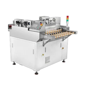
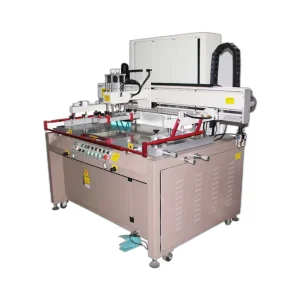
Application: for PCB Bard Board Or Film Inspecting
| Item | Detail |
|---|---|
| Technology Range | Down to 1.2 mil (30 µm) line & space |
| Products Inspected | Inner layers: Signal, power & ground, mixed, cross shielding, inner with holes, buildup, Outer layers: Signal, mixed, cross shielding, buildup Build-up layers: Laservias (conformal and non-conformal masks |
| Materials Inspected | Conventional: Bare copper (shiny, matte), etched additive or plated copper, reverse treated foil (RTF), doubletreated copper, gold-plated conductors. Any laminate including FR4, Tetra function, Teflon, Roger etc. Flex material: Polyimide, polyester Advanced build-up board materials: Any laminate including RCC Photoresist: Blue, purple & brown |
| Defects Detected | Shorts, opens, minimum line/space violations, nicks, protrusions, dishdowns, copper splashes, pinholes, missing or excess features, wrong size and position of features, clearance and split plane violations, blocked holes, annular ring violations, SMT violations. |
| Inspection Method | Shorts, opens, minimum line/space violations, nicks, protrusions, dishdowns, copper splashes, pinholes, missing or excess features, wrong size and position of features, clearance and split plane violations, blocked holes, annular ring violations, SMT violations. |
| Panel Dimensions | Thickness range: 1-300 mil (25-7500 µm) Max. Panel size/ Inspected area: 26” x 24” (660 x 610 mm) Max. Panel size/ Inspected area with large table: 26” x 31” (660 x 787mm) |
| Setup Data Sources | CAM |


Reviews
There are no reviews yet.