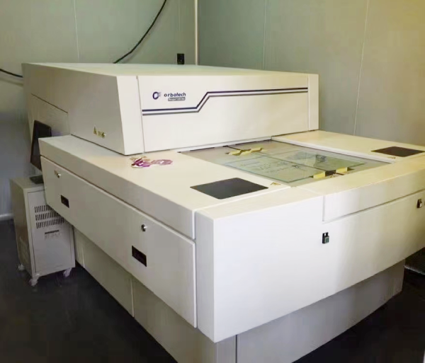
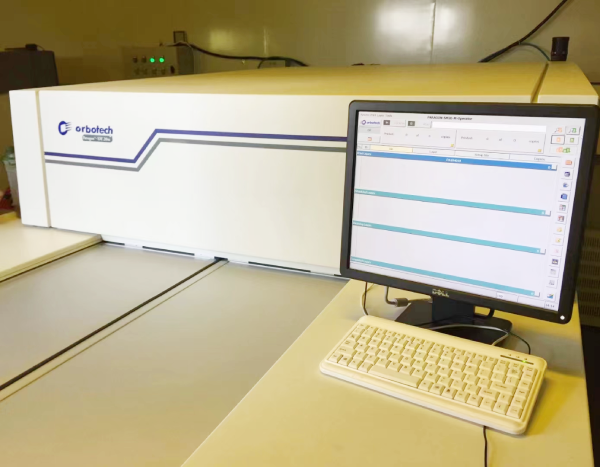
Application: Laser Direct Imaging Machine for PCB (Orbotech Brand)
| Артикул | Размер |
|---|---|
| Модель: | Paragon-SM 20 |
| Resolutions: | 8000 точек на дюйм |
| Throughput*(max. prints/hour 18" x 24"): | @10mJ/cm2 SR: 160 @100mJ/cm2 SR: 80 |
| Minimum Feature Size: | 1mil |
| Edge Roughness: | +/-0.1mil |
| Exposure Wavelength: | UV Range, 355nm, 16W |
| Energy Range (mJ/cm2): | 10-2200 |
| Positioning Accuracy (FTG): | +/-0.5mil |
| Side-to-Side Registration: | 1mil |
| Max. Substrate Size: | 25*32'' |
| Max. Exposure Area: | 24*32'' |
| Substrate Thickness: | 0.001''-0.315'' |
| Applications: | Solder mask/Inner layers and outer layers/Sequential build-up layers/Flex and Rigid-Flex PCBs |






Отзывы
Отзывов пока нет.