

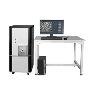
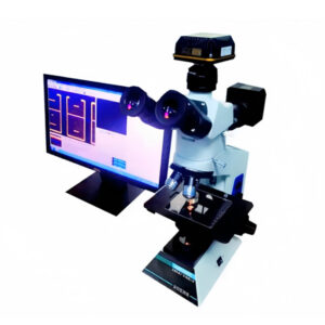
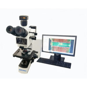
Application: Desktop SEM microscope supports PCB failure analysis to detect delamination, circuit corrosion and micro structural abnormalities efficiently. (New Machine)
| Παράμετρος | Specification |
|---|---|
| Magnification | 60,000×/150,000× (optional) |
| Accelerating Voltage | 5–30 kV (5/10/15/20/30 kV selectable) |
| Resolution | 15 nm (30 kV, SE); 20 nm (30 kV, BSE) |
| Imaging | SE, BSE, Multi (SE+BSE) |
| Detector | SE / BSE |
| Vacuum | High / Low (reduces sample prep) |
| Options | EDS (elemental analysis), CCD camera (stage view) |
| Stage Control | Manual / Automatic |
| Auto Functions | Startup, Focus, Brightness/Contrast |
| Image Formats | BMP, JPEG, PNG, TIFF |
| Software | Image edit/save, length/area/angle measurement |
| On-image info | Mag, KV, detector, scale bar, date/time |
Αξιολογήσεις
Δεν υπάρχει καμία αξιολόγηση ακόμη.